Superfine production process and modification process of silicon micropowder for copper clad laminate
Copper Clad Laminate (CCL for short) is an electronic basic material made by impregnating glass fiber cloth or other reinforcing materials with a resin matrix, covering one or both sides with copper foil and hot pressing. Used in communication equipment, consumer electronics, computers, automotive electronics, industrial control medical, aerospace and other fields. The choices of fillers for CCL include silica powder, aluminum hydroxide, magnesium hydroxide, talc powder, mica powder and other materials.
Silicon micropowder has relative advantages in heat resistance, mechanical properties, electrical properties and dispersibility in the resin system. It can be used to improve heat resistance and humidity resistance, thin CCL rigidity, dimensional stability, and drilling positioning accuracy The smoothness of the inner wall, the adhesion between the layers or the insulating layer and the copper foil, and the reduction of the thermal expansion coefficient.
Types of silicon powder for copper clad laminates
At present, the silicon powder used in integrated circuit copper clad laminates mainly includes five varieties: crystalline silicon powder, molten (amorphous) silicon powder, spherical silicon powder, composite silicon powder, and active silicon powder.
- Crystalline silica powder
Started early, the process is mature and simple, and the price is relatively cheap. It has a great effect on the improvement of the rigidity, thermal stability and water absorption of the copper clad laminate.
The impact on the resin system is not optimal, the dispersibility and sedimentation resistance are not as good as the molten spherical silicon powder, the impact resistance is not as good as the molten transparent silicon powder, the thermal expansion coefficient is high, and the hardness is large, and the processing is difficult.
- Fused silica powder
White color, high purity, low linear expansion coefficient, low stress, is mainly used in large-scale and ultra-large-scale integrated circuit molding compound, epoxy castable and potting compound, especially in the application of high-frequency copper clad laminates. .
The higher melting temperature requires higher production capacity of the enterprise, complicated process and higher production cost. Generally, the dielectric constant of the product is too high, which affects the signal transmission speed.
- Spherical silica powder
The fluidity is good, the filling rate in the resin is high, the internal stress is low, the size is stable, the thermal expansion coefficient is low after being made into the plate, and it has a high bulk density and uniform stress distribution, so it can increase the fluidity and Reduce viscosity.
The price is very high and the process is complicated. At present, it has not been used on a large scale in the copper clad laminate industry, and a small amount is used in the fields of integrated circuit carrier boards and printed circuit boards.
- Compound silicon powder
Good temperature resistance, good acid and alkali corrosion resistance, poor thermal conductivity, high insulation, low expansion, stable chemical properties; moderate hardness, easy to process, reduce the wear of the drill bit in the drilling process, and reduce the dust pollution during the drilling process .
If the performance of the copper clad laminate can be guaranteed, the cost needs to be reduced.
- Active silica powder
Good temperature resistance, good acid and alkali corrosion resistance, poor thermal conductivity, high insulation, low expansion, stable chemical properties, and high hardness.
The resin systems used by copper clad laminate manufacturers are not the same. It is difficult for the silicon powder manufacturers to make the same product suitable for all users’ resin systems, and the copper clad laminate manufacturers are more willing to add modifiers themselves due to their habits.
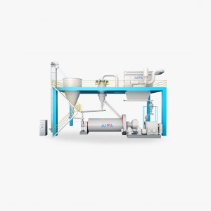
Production process of ultra-fine silicon powder
As electronic products become lighter, thinner, shorter and smaller, the use of silicon micropowder filler in copper clad laminates also requires more and more ultra-fineness. The chemical synthesis method of ultra-fine silicon powder has low yield and complex process. The physical pulverization method has low cost, simple process, and is suitable for mass industrial production. The pulverization method is divided into a dry process and a wet process.
- Dry process
The process is feeding→grinding→classification→collection→packaging. The process is simple and the production cost is low. Generally, silicon powder production enterprises choose this process.
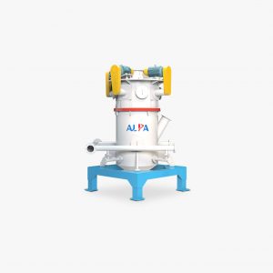
Grinding and classification equipment is the key. The grinding equipment mainly uses ball mills. The energy consumption of the ball mill is relatively low and the production capacity is large. For some products with higher purity requirements, the jet mill can be used because the jet mill does not introduce the grinding medium, but the energy consumption of the jet mill is relatively high. Low. The classification equipment is a general air flow classifier.
- Wet process
The process is feeding→grinding→drying→deaggregation→classification→collection→packaging. Drying and deaggregation processes are required. The process is complicated and the production cost is high. Fewer companies adopt this process. The cut point is less than 5 microns and requires a surface. This process is more suitable for processing products.
In fact, for the same process, the finer the particle size of the product, the lower the cut point, the higher the energy consumption, the lower the productivity, the more serious the equipment wear, the more obvious the increase in production costs, and the higher the cost.
Surface modification of ultra-fine silicon powder
The surface modification of ultra-fine silicon powder can reduce the interaction between particles, effectively prevent particle agglomeration, reduce the viscosity of the entire system, and increase the fluidity of the system; it can enhance the compatibility of the particles with the resin matrix and make the filler particles It can be evenly dispersed in the glue.
The key to surface modification lies in how to make the modifier uniformly dispersed on the surface of the particles while ensuring the chemical bonding conditions between the modifier and the particle surface.
The dry modification process is relatively simple and the production cost is relatively low, but the effect is relatively poor. The wet process has a better modification effect, but the process is complex, requires drying and depolymerization processes, and the production cost is high.
For conventional copper clad laminates with silicon powder, dry modification is generally recommended. For 8μm cut and 6μm cut comprehensive cost and performance considerations, dry process is recommended. For products with a cut of 5μm and below, a wet process is recommended. For finer products, gas phase synthesis has been used for surface modification.
With the continuous deepening of copper clad laminate manufacturers’ understanding of silicon micropowder, new requirements are also put forward for the impurities of silicon micropowder. This is mainly because the silicon micropowder impurity affects the appearance, insulation and heat resistance of the PP and substrate of CCL. Come negatively. Silicon powder impurities can be divided into two categories: magnetic impurities and non-magnetic impurities according to whether they are magnetic or not.
The key to impurity control is to ensure that the raw material impurities are sufficiently low; to prevent the environment from being introduced during the production process; to prevent the equipment and pipes from wearing out; to remove impurities during the production process (using a magnetic separator to remove magnetic impurities, which is difficult to remove non-magnetic impurities).
The future trends of fillers for copper clad laminates are as follows:
- Functionalization: Low Dk, Low Df, high thermal conductivity, flame retardant, etc.
- High filling: High filling means better performance of inorganic fillers, including low CTE, low dielectric, and high thermal conductivity.
- Particle design: Interface and agglomeration issues require continuous improvement in surface treatment technology; spherical products are the choice for high-end applications.
- Particle size distribution design: In response to the thinning, the particle size needs to be continuously reduced, but it is also necessary to prevent the difficulty of dispersion.
- Impurity control: Ultra-thin, highly reliable, and highly thermally conductive substrates expect the impurity content of the filler to be as low as possible.
Article source: China Powder Network